- 您现在的位置:买卖IC网 > Sheet目录2000 > IDT82V3011PVG (IDT, Integrated Device Technology Inc)IC PLL WAN T1/E1/OC3 SGL 56-SSOP
IDT and the IDT logo are trademarks of Integrated Device Technology, Inc.
2006 Integrated Device Technology, Inc.
DSC-6237/5
1
May 24, 2006
T1/E1/OC3 WAN PLL WITH
SINGLE REFERENCE INPUT
IDT82V3011
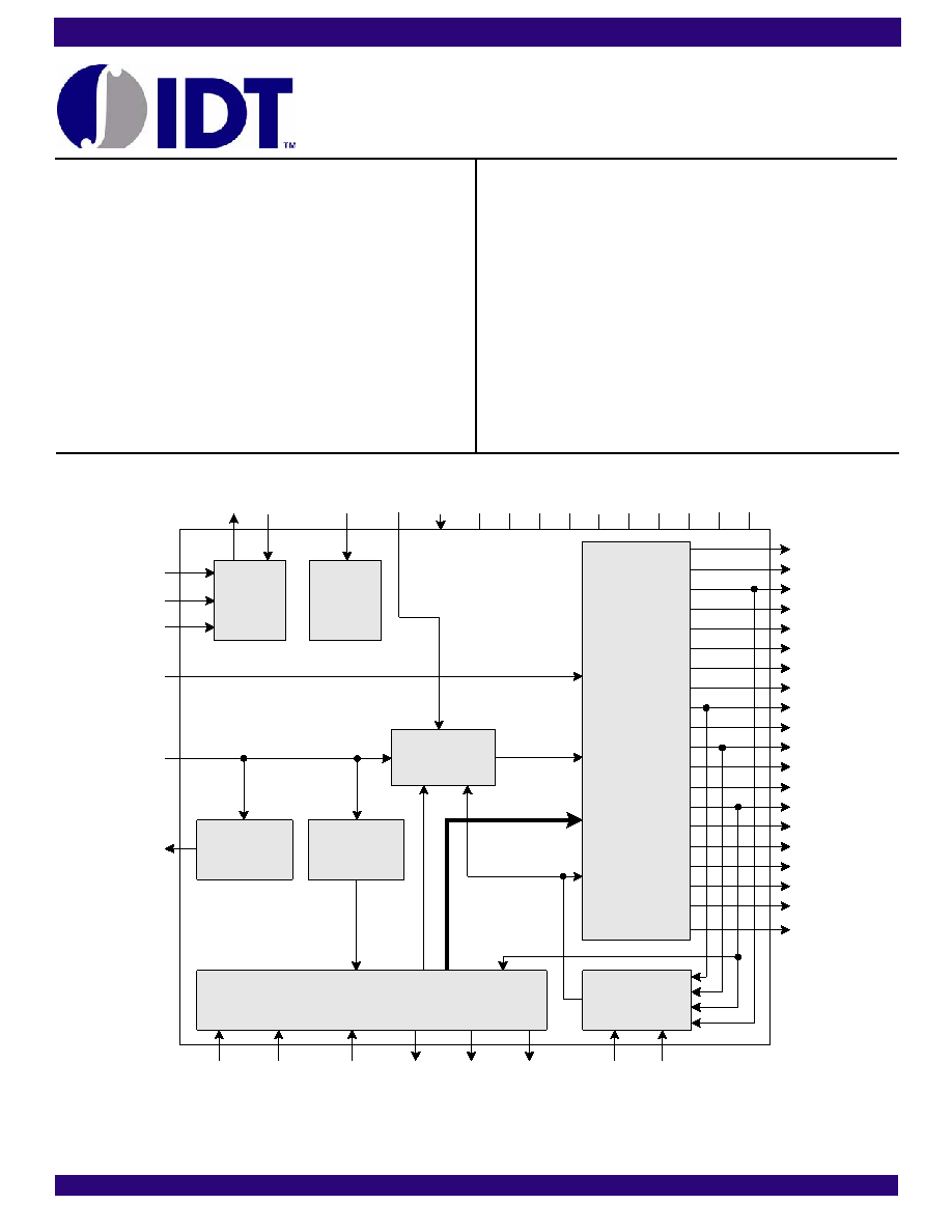
FUNCTIONAL BLOCK DIAGRAM
TIE Control
Block
Input Frequency
Selection
F_sel0
F_sel1
Freerun
Normal Holdover
Fref
FLOCK
Invalid Input
Signal
Detection
MODE_sel0
MODE_sel1
TIE_en
Virtual
Reference
Feedback Signal
C16o
C8o
C4o
C2o
C3o
C1.5o
F0o
F8o
F16o
RSP
TSP
F19o
C6o
LOCK
F32o
C19POS
C19NEG
OSC
OSCi
TCLR
V
DDD
V
SS
V
SS
TDO TDI
JTAG
TMS
TRST
TCK
V
DDD
V
SS
V
DDD
V
DDA VSS
RST
State Control Circuit
Reference
Input Monitor
MON_out
C32o
C19o
DPLL
C2/C1.5
V
DDA VSS
FEATURES
Supports AT&T TR62411 and Telcordia GR-1244-CORE Stratum
4 Enhanced and Stratum 4 timing for DS1 interfaces
Supports ETSI ETS 300 011, TBR 4, TBR 12 and TBR 13 timing
for E1 interface
Selectable input reference: 8 kHz, 1.544 MHz, 2.048 MHz or 19.44
MHz
Provides C1.5o, C3o, C2o, C4o, C6o, C8o, C16o, C19o and C32o
output clock signals
Provides 7 types of 8 kHz framing pulses: F0o, F8o, F16o, F19o,
F32o, RSP and TSP
Provides a C2/C1.5 output clock signal with the frequency
controlled by the reference input Fref
Holdover frequency accuracy of 0.025 ppm
Phase slope of 5 ns per 125 s
Attenuates wander from 2.1 Hz
Fast lock mode
Provides Time Interval Error (TIE) correction
MTIE of 600 ns
JTAG boundary scan
Holdover status indication
Freerun status indication
Normal status indication
Lock status indication
Input reference quality indication
3.3 V operation with 5 V tolerant I/O
Package available: 56-pin SSOP (Green option available)
发布紧急采购,3分钟左右您将得到回复。
相关PDF资料
IDT82V3012PVG8
IC PLL WAN T1/E1/OC3 DUAL 56SSOP
IDT82V3155PVG
IC PLL WAN T1/E1/OC3 DUAL 56SSOP
IDT82V3202NLG
IC PLL WAN EBU SGL 68-VFQFPN
IDT82V3255TFG
IC PLL WAN SMC STRATUM 3 64-TQFP
IDT82V3280APFG
IC PLL WAN SE STRATUM 2 100TQFP
IDT82V3285AEQG
IC PLL WAN SE STRATUM 100TQFP
IDT82V3285EQG
IC PLL WAN SE STRATUM 100TQFP
IDT82V3288BCG
IC PLL WAN 3E STRATUM 2 208CABGA
相关代理商/技术参数
IDT82V3011PVG8
功能描述:IC PLL WAN T1/E1/OC3 SGL 56-SSOP RoHS:是 类别:集成电路 (IC) >> 时钟/计时 - 专用 系列:- 标准包装:1,500 系列:- 类型:时钟缓冲器/驱动器 PLL:是 主要目的:- 输入:- 输出:- 电路数:- 比率 - 输入:输出:- 差分 - 输入:输出:- 频率 - 最大:- 电源电压:3.3V 工作温度:0°C ~ 70°C 安装类型:表面贴装 封装/外壳:28-SSOP(0.209",5.30mm 宽) 供应商设备封装:28-SSOP 包装:带卷 (TR) 其它名称:93786AFT
IDT82V3012
制造商:IDT 制造商全称:Integrated Device Technology 功能描述:T1/E1/OC3 WAN PLL WITH DUAL REFERENCE INPUTS
IDT82V3012PV
制造商:Integrated Device Technology Inc 功能描述:
IDT82V3012PVG
功能描述:IC PLL WAN T1/E1/OC3 DUAL 56SSOP RoHS:是 类别:集成电路 (IC) >> 时钟/计时 - 专用 系列:- 标准包装:1 系列:- 类型:时钟/频率发生器,多路复用器 PLL:是 主要目的:存储器,RDRAM 输入:晶体 输出:LVCMOS 电路数:1 比率 - 输入:输出:1:2 差分 - 输入:输出:无/是 频率 - 最大:400MHz 电源电压:3 V ~ 3.6 V 工作温度:0°C ~ 85°C 安装类型:表面贴装 封装/外壳:16-TSSOP(0.173",4.40mm 宽) 供应商设备封装:16-TSSOP 包装:Digi-Reel® 其它名称:296-6719-6
IDT82V3012PVG8
功能描述:IC PLL WAN T1/E1/OC3 DUAL 56SSOP RoHS:是 类别:集成电路 (IC) >> 时钟/计时 - 专用 系列:- 标准包装:1,500 系列:- 类型:时钟缓冲器/驱动器 PLL:是 主要目的:- 输入:- 输出:- 电路数:- 比率 - 输入:输出:- 差分 - 输入:输出:- 频率 - 最大:- 电源电压:3.3V 工作温度:0°C ~ 70°C 安装类型:表面贴装 封装/外壳:28-SSOP(0.209",5.30mm 宽) 供应商设备封装:28-SSOP 包装:带卷 (TR) 其它名称:93786AFT
IDT82V3155
制造商:IDT 制造商全称:Integrated Device Technology 功能描述:ENHANCED T1/E1/OC3 WAN PLL WITH DUAL REFERENCE INPUTS
IDT82V3155PV
制造商:IDT 制造商全称:Integrated Device Technology 功能描述:ENHANCED T1/E1/OC3 WAN PLL WITH DUAL REFERENCE INPUTS
IDT82V3155PVG
功能描述:IC PLL WAN T1/E1/OC3 DUAL 56SSOP RoHS:是 类别:集成电路 (IC) >> 时钟/计时 - 专用 系列:- 标准包装:1,500 系列:- 类型:时钟缓冲器/驱动器 PLL:是 主要目的:- 输入:- 输出:- 电路数:- 比率 - 输入:输出:- 差分 - 输入:输出:- 频率 - 最大:- 电源电压:3.3V 工作温度:0°C ~ 70°C 安装类型:表面贴装 封装/外壳:28-SSOP(0.209",5.30mm 宽) 供应商设备封装:28-SSOP 包装:带卷 (TR) 其它名称:93786AFT